P-GaN E-mode JFET Technology
Introduction
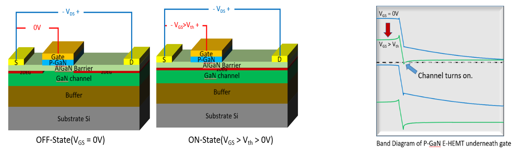
Due to high electron concentration in the quantum well of AlGaN/GaN heterojunction, the GaN HEMT is inherently a normally-on (or depletion-mode) device. Many efforts were made in the literature to remove the electrons under the gate for forming a normally-off device.
One of the successful approaches is the use of a p-GaN cap layer atop the AlGaN/GaN HEMT, in specific in the location of gate metal. With the device structure, the 2DEG under the gate can be completely depleted, which means the P-GaN-capped HEMT device can be operated in an enhancement mode (E-mode).
Besides, the cross-sectional structure under the gate is primarily composed of p-GaN (p), intrinsic AlGaN (i), and n-channel GaN (n) layers, and therefore the device is usually called p-GaN E-mode Junction FET (JFET). Threshold voltages of the p-GaN E-mode JFET are typically around 1~2V. For turning on the device, gate bias needs to be applied beyond the threshold voltage for having current flowing in the channel, as shown in the schematics below.
Advantage
Low capacitances (Ciss, Coss, Crss…)、gate charge (Qg)、switching times (tD(on), tR, tD(off), tF) and zero reverse recovery time/charge (trr/Qrr): Fast switching frequency、low switching loss、high conversion efficiency.
Easy monolithic integration with Si devices or IC.
Easy monolithic integration with Si devices or IC.