Super Junction MOSFET Wafer

Super Junction Wafer
 

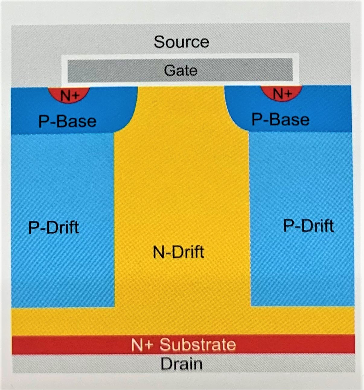
The Super Junction MOSFET structure can get lower on-resistance and chip area than traditional VDMOS MOSFET.
It is primarily used for high-VDSS MOSFETS.


P/N Status VDSS(V) VGSS(V) ID(A) Type VGS(th)
Min(V)
VGS(th)
Max(V)
RDS(ON)
Typ.mΩ
RDS(ON)
Max.mΩ
Gross Die Chip Size
(without S/L)
X(mm)
Chip Size
(without S/L)
Y(mm)
Remark
MP600D820 MP 600 ±30 6 N-type 2.8 4.2 750 840 6108 2.281 1.911
MP600D500 MP 600 ±30 8 N-type 2.8 4.2 480 550 4341 2.713 2.261
MP600D320 MP 600 ±30 11 N-type 2.8 4.2 305 330 3033 3.121 2.811
MP600D300 MP 600 ±30 13 N-type 2.8 4.2 250 300 2678 3.481 2.861
MP600D200 MP 600 ±30 15 N-type 2.8 4.2 180 210 2007 4.021 3.301
MP600D140 MP 600 ±30 24 N-type 2.8 4.2 120 150 1409 4.777 3.901
MP600D080 MP 600 ±30 47 N-type 2.8 4.2 72 90 878 6.049 4.921
MP650D900 MP 650 ±30 5 N-type 2.8 4.2 748 850 6108 2.281 1.911
MP650D550 MP 650 ±30 8 N-type 2.8 4.2 500 550 4341 2.713 2.261
MP650D350 MP 650 ±30 11 N-type 2.8 4.2 318 350 3033 3.121 2.811
MP650D220 MP 650 ±30 15 N-type 2.8 4.2 190 220 2007 4.021 3.301
MP650D150 MP 650 ±30 24 N-type 2.8 4.2 140 170 1409 4.777 3.901
MP650D090 MP 650 ±30 47 N-type 2.8 4.2 72 90 878 6.049 4.921
MP650D055 MP 650 ±30 54 N-type 2.8 4.2 56 68 650 6.887 5.841

Contact us for cooperation.